- 您现在的位置:买卖IC网 > Sheet目录17338 > ISL8201MEVAL1Z (Intersil)BOARD EVAL STEP-DOWN POL ISL8201
�� �
�
�ISL8201M�
�the� soft-start� ramps� begins.� This� prevents� a� disturbance� on�
�the� output,� due� to� the� internal� regulator� turning� on� or� off.� If� the�
�transition� is� slow� (not� a� step� change),� the� disturbance� should�
�be� minimal.� Thus,� while� the� recommendation� is� to� not� have�
�the� output� enabled� during� the� transition� through� this� region,� it�
�the� capacitor,� the� less� ripple� expected� but� consideration�
�should� be� taken� for� the� higher� surge� current� during�
�power-up.� The� ISL8201M� provides� the� soft-start� function� that�
�controls� and� limits� the� current� surge.� The� value� of� the� input�
�capacitor� can� be� calculated� by� Equation� 5:�
�C� IN� =� -------------------�
�may� be� acceptable.� The� user� should� monitor� the� output� for�
�their� application� to� see� if� there� is� any� problem.� If� P� VCC� powers�
�I� IN� ×� Δ� t�
�Δ� V�
�(EQ.� 5)�
�up� first� and� the� V� IN� is� not� present� by� the� time� the� initialization�
�is� done,� then� the� soft-start� will� not� be� able� to� ramp� the� output,�
�and� the� output� will� later� follow� part� of� the� V� IN� ramp� when� it� is�
�applied.� If� this� is� not� desired,� then� change� the� sequencing� of�
�the� supplies,� or� use� the� COMP/EN� pin� to� disable� V� OUT� until�
�both� supplies� are� ready.�
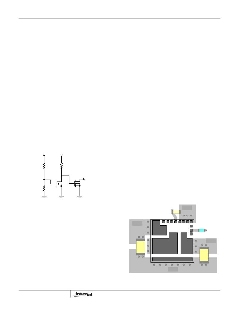
�Figure� 20� shows� a� simple� sequencer� for� this� situation.� If�
�P� VCC� powers� up� first,� Q� 1� will� be� off,� and� R� 3� pulling� to� P� VCC�
�will� turn� Q� 2� on,� keeping� the� ISL8201M� in� shut-down.� When�
�V� IN� turns� on,� the� resistor� divider� R� 1� and� R� 2� determines� when�
�Q� 1� turns� on,� which� will� turn� off� Q� 2� and� release� the�
�shut-down.� If� V� IN� powers� up� first,� Q� 1� will� be� on,� turning� Q� 2�
�off;� so� the� ISL8201M� will� start-up� as� soon� as� P� VCC� comes�
�up.� The� V� ENDIS� trip� point� is� 0.4V� nominal,� so� a� wide� variety�
�of� N-MOSFET� or� NPN� BJT� or� even� some� logic� IC's� can� be�
�used� as� Q� 1� or� Q� 2� .� However,� Q� 2� must� be� low� leakage� when�
�off� (open-drain� or� open-collector)� so� as� not� to� interfere� with�
�the� COMP� output.� Q� 2� should� also� be� placed� near� the�
�COMP/EN� pin.�
�Where:�
�C� IN� is� the� input� capacitance� (μF)�
�I� IN� is� the� input� current� (A)�
�Δ� t� is� the� turn� on� time� of� the� high-side� switch� (μs)�
�Δ� V� is� the� allowable� peak-to-peak� voltage� (V)�
�In� addition� to� the� bulk� capacitance,� some� low� Equivalent�
�Series� Inductance� (ESL)� ceramic� capacitance� is�
�recommended� to� decouple� between� the� drain� terminal� of� the�
�high� side� MOSFET� and� the� source� terminal� of� the� low� side�
�MOSFET.� This� is� used� to� reduce� the� voltage� ringing� created�
�by� the� switching� current� across� parasitic� circuit� elements.�
�Output� Capacitors�
�The� ISL8201M� is� designed� for� low� output� voltage� ripple.� The�
�output� voltage� ripple� and� transient� requirements� can� be� met�
�with� bulk� output� capacitors� (C� OUT� )� with� low� enough�
�Equivalent� Series� Resistance� (ESR).� C� OUT� can� be� a� low�
�V� IN�
�R1�
�R3�
�PVCC�
�TO� COMP/EN�
�ESR� tantalum� capacitor,� a� low� ESR� polymer� capacitor� or� a�
�ceramic� capacitor.� The� typical� capacitance� is� 330μF� and�
�decoupled� ceramic� output� capacitors� are� used.� The�
�internally� optimized� loop� compensation� provides� sufficient�
�stability� margins� for� all� ceramic� capacitor� applications� with� a�
�recommended� total� value� of� 400μF.� Additional� output� filtering�
�may� be� needed� if� further� reduction� of� output� ripple� or�
�dynamic� transient� spike� is� required.�
�R2�
�Q1�
�Q2�
�Layout� Guide�
�To� achieve� stable� operation,� low� losses,� and� good� thermal�
�performance� some� layout� considerations� are� necessary.�
�FIGURE� 20.� SEQUENCE� CIRCUIT�
�The� V� IN� range� can� be� as� low� as� ~1V� (for� V� OUT� as� low� as� the�
�0.6V� reference)� and� as� high� as� 20V.� There� are� some�
�C� PVCC�
�PGND�
�restrictions� for� running� high� V� IN� voltage.� The� maximum�
�PHASE� voltage� is� 30V.� The� VIN� +� P� VCC� +� any� ringing� or�
�other� transients� on� the� PHASE� pin� must� be� less� than� 30V.� If�
�V� IN� is� 20V,� it� is� recommended� to� limit� P� VCC� to� 5V.�
�V� IN�
�R� FB�
�Switching� Frequency�
�The� switching� frequency� is� a� fixed� 600kHz� clock,� which� is�
�determined� by� the� internal� oscillator.� However,� all� of� the� other�
�timing� mentioned� (POR� delay,� OCP� sample,� soft-start,� etc.)� is�
�independent� of� the� clock� frequency� (unless� otherwise� noted).�
�Selection� of� the� Input� Capacitor�
�The� input� filter� capacitor� should� be� based� on� how� much�
�ripple� the� supply� can� tolerate� on� the� DC� input� line.� The� larger�
�12�
�C� IN�
�V� OUT�
�C� OUT1�
�(DECOUPLE)�
�PGND�
�FIGURE� 21.� RECOMMENDED� LAYOUT�
�FN6657.2�
�October� 21,� 2010�
�发布紧急采购,3分钟左右您将得到回复。
相关PDF资料
EEC15DREI-S13
CONN EDGECARD 30POS .100 EXTEND
RCM15DCSH-S288
CONN EDGECARD 30POS .156 EXTEND
EEC20DREH-S13
CONN EDGECARD 40POS .100 EXTEND
RCC07DRXI
CONN EDGECARD 14POS DIP .100 SLD
594D106X9020B8T
CAP TANT 10UF 20V 10% 1611
TARS226M010
CAP TANT 22UF 10V 20% AXIAL
EBC15DCMI
CONN EDGECARD 30POS .100 WW
A9BAG-1606F
FLEX CABLE - AFF16G/AF16/AFE16T
相关代理商/技术参数
ISL8201MIRZ
功能描述:DC/DC转换器 STAND ALONE 10A DC/D CSTEPDWNPWRSUPPYMOD1
RoHS:否 制造商:Murata 产品: 输出功率: 输入电压范围:3.6 V to 5.5 V 输入电压(标称): 输出端数量:1 输出电压(通道 1):3.3 V 输出电流(通道 1):600 mA 输出电压(通道 2): 输出电流(通道 2): 安装风格:SMD/SMT 封装 / 箱体尺寸:
ISL8201MIRZ-T
功能描述:DC/DC转换器 ST& ALONE 10A DC/DC DWN PWR SUPPLY MOD RoHS:否 制造商:Murata 产品: 输出功率: 输入电压范围:3.6 V to 5.5 V 输入电压(标称): 输出端数量:1 输出电压(通道 1):3.3 V 输出电流(通道 1):600 mA 输出电压(通道 2): 输出电流(通道 2): 安装风格:SMD/SMT 封装 / 箱体尺寸:
ISL8204M
制造商:INTERSIL 制造商全称:Intersil Corporation 功能描述:Complete High Efficiency DC/DC Power Module
ISL8204MEVAL1Z
功能描述:电源管理IC开发工具 ISL8204 EVAL BRD 1 ROHS CMPL MOD
RoHS:否 制造商:Maxim Integrated 产品:Evaluation Kits 类型:Battery Management 工具用于评估:MAX17710GB 输入电压: 输出电压:1.8 V
ISL8204MIRZ
功能描述:DC/DC转换器 STAND ALONE 4A DC/DC STEPDWNPWRSUPPYMOD15
RoHS:否 制造商:Murata 产品: 输出功率: 输入电压范围:3.6 V to 5.5 V 输入电压(标称): 输出端数量:1 输出电压(通道 1):3.3 V 输出电流(通道 1):600 mA 输出电压(通道 2): 输出电流(通道 2): 安装风格:SMD/SMT 封装 / 箱体尺寸:
ISL8204MIRZ-T
功能描述:DC/DC转换器 ST& ALONE 4A DC/DC DWN PWR SUPPLY MOD RoHS:否 制造商:Murata 产品: 输出功率: 输入电压范围:3.6 V to 5.5 V 输入电压(标称): 输出端数量:1 输出电压(通道 1):3.3 V 输出电流(通道 1):600 mA 输出电压(通道 2): 输出电流(通道 2): 安装风格:SMD/SMT 封装 / 箱体尺寸:
ISL8206M
制造商:INTERSIL 制造商全称:Intersil Corporation 功能描述:Complete High Efficiency DC/DC Power Module
ISL8206MEVAL1Z
功能描述:电源管理IC开发工具 ISL8206 EVAL BRD 1 ROHS CMPL MOD
RoHS:否 制造商:Maxim Integrated 产品:Evaluation Kits 类型:Battery Management 工具用于评估:MAX17710GB 输入电压: 输出电压:1.8 V